Services
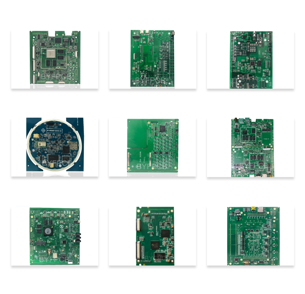
In a typical printed‑circuit‑board assembly (PCBA) process for an IoT device, the following stages are key:
-
1. Design verification and preparation – Engineers finalize the schematic, component layout and bill of materials for the IoT PCB. They verify the design using design‑for‑manufacture (DFM) checks to ensure component clearances, signal integrity and power considerations are met.
-
2. Component sourcing – The required components—microcontrollers, wireless modules, sensors, power‑management ICs, connectors and passive parts—are procured. Because IoT devices rely on miniaturized, low‑power parts and wireless modules, sourcing components that meet size, efficiency and reliability requirements is critical.
-
3. PCB fabrication – The bare PCBs are produced by etching copper traces onto an insulating substrate. For IoT devices this often involves multilayer or high‑density interconnect boards to accommodate miniature footprints and multiple functions.
-
4. Solder paste printing – A stencil is used to apply solder paste onto the pads where surface‑mount components will be placed.
-
5. Pick‑and‑place assembly – Automated equipment places microcontrollers, wireless modules, sensors and other components onto the board. Surface‑mount technology (SMT) allows for the small, lightweight assemblies used in IoT devices.
-
6. Reflow soldering – The assembly passes through a controlled oven that melts the solder paste and bonds the components to the board.
-
7. Through‑hole assembly (if required) – Larger connectors or other through‑hole parts are inserted and soldered manually or by wave soldering.
-
8. Inspection and quality testing – Assemblies undergo automated optical inspection (AOI), X‑ray inspection and sometimes in‑circuit testing to check for solder joint integrity, shorts and opens. Functional testing ensures the microcontroller, sensors and wireless modules operate correctly. Proper thermal management and signal integrity are verified, because IoT PCBs must handle heat and electromagnetic interference effectively.
-
9. Programming and final test – Firmware is loaded onto the microcontroller, and the completed device is tested for connectivity (e.g., Wi‑Fi or Bluetooth), sensor accuracy and power consumption. Security features such as encryption modules or secure elements may also be tested.
-
10. Conformal coating and enclosure assembly – If the device needs protection from moisture or dust, a conformal coating is applied. The PCB is then integrated into its housing, and final quality checks are performed.
These steps ensure that an IoT device’s PCB is manufactured to professional standards—optimized for size, power efficiency and reliability while integrating sensors, microcontrollers and wireless communication modules essential to IoT functionality.